Home
About
Products
Application
Laser Knowledge
Contact Us
Contact us
home page>Products>Sistemas de micro mecanizado>Sistema de marcado láser de obleas/laminas
RETURN
Sistema de marcado láser de obleas/laminas
Wafer laser marking machine.
Laser marking is widely used in the semiconductor industry due to its apparent advantages, such as high marking accuracy, fast speed, and permanent marking.
Wafer marking on the die requires good marking quality. High cleanliness levels will ensure traceability and reliability.
Contact us
Características
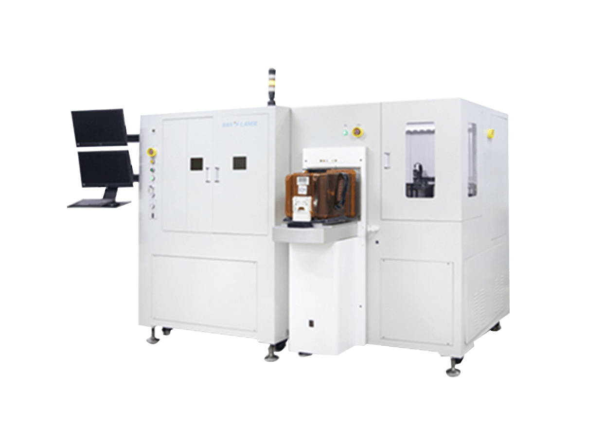
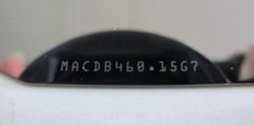
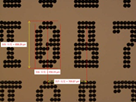
A laser is used to print the lot number (such as ABC1234) directly above the wafer to ensure the entire process chain's traceability. This lot number is composed of many recessed holes. There may be some derivatives after marking, which will accumulate around the pits. Excessive or hard protrusions may scratch the wafer's surface in the later process and cause the wafer to be scrapped. Ultraviolet laser processing is a cold processing method that solves accumulation, making it an ideal wafer marking program.
 
- Automatic wafer pick-up from the magazine
- Finding wafers automatically with edge seeker 
- Automatic positioning marking with the visual system
- The visual inspection system is available
- Available to mark on the backside of the wafer through the transmittance film 
- Complies with the SMEMA standard
- SMIF and other automatic loading and unloading modules can be selected as an extension
- UV and Green laser modules can be selected upon to the demand
______________________________________________________________________________________
 
                        
Application and Samples
6-inch, 8-inch, 12-inch wafer front or back marking
Technical Specs
 
Laser Type UV Laser
Wavelength 355 nm 
Min Beam Diameter  < 10 µm
Beam Quality M2 < 1.2
Pulse Frequency 10 - 200 kHz
Output Power 10 Watts
Repetition Accuracy 2 μm
Cooling System Water-cooled
Fθ Marking Field Size 1.96" x 1.96" (50mm x 50mm)
X, Y travel Distance 15.74" x 11.81" (400mm x 300 mm)
Laser Safety Level Class I
Electrical Connection 110 - 230 V (± 10%) 20 A, 50/60 Hz
Power Consumed 5 Kw
Warranty Coverage(Parts & Labor) 1-year
Laser Safety Compliance FDA(CDRH)
Running Temperature 15℃-35℃ / 59°-95°F


Options and Accessories
SMIF, other automatic loading and unloading modules
SOBRE HAN´S LASER CORPORATION
Han's Laser Corporation es una subsidiaria de propiedad absoluta de Han's Laser Technology Group, un líder mundial en tecnología láser industrial. Estamos comprometidos a brindar a nuestros clientes la última tecnología de máquinas láser industriales para satisfacer mejor sus necesidades particulares.

Con sede en los EE. UU., conformado por personal capacitado y experto. Han's Laser está transformando la industria con nuestras máquinas de última generación. Han's Laser Technology Industry Group Co., Ltd, una empresa pública establecida en 1996, se ha convertido en el buque insignia de la industria láser nacional china y un reconocido fabricante de equipos láser del mundo. Han's Laser comenzó a cotizarse en la Bolsa de Valores de Shenzhen en 2004. Y a día de hoy, su valor de mercado alcanza más de 7 mil millones de dólares.